
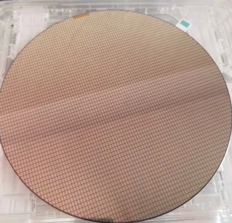
Qitai Semiconductor has the CP (circuit probe) testing service capability for 6-12 inch wafers, providing customized CP testing support for complex large-scale SoC chips, RF and communication chips, analog and mixed signal chips and other chip product wafers.
Product features:
- Wafer testing: 12 inch, 8 inch, 6 inch wafer testing.
- Trial scope: including advanced processes such as 17nm, 22nm, 28nm, and all mature processes of wafers above 28nm.
- Test business process: requirement mining → service module construction → service scheme design → scheme implementation and feedback → service delivery completion.
- Testing process flow: testing plan evaluation → outsourcing needle card production → LB production → testing program development → machine debugging → data confirmation → mass production → providing customer testing reports and data → shipment